President Lee unveiled an 800 trillion won ($520B) public-private plan for four new Samsung and SK Hynix fabs, dwarfing the US CHIPS Act tenfold.
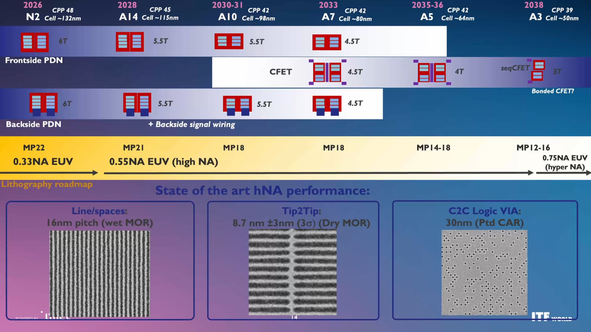
As CPP shrinking stalls, chipmakers find a new way to increase transistor density. Imec foresees 0.3nm in 2038, CFET insertion in 2038, HLSI era.
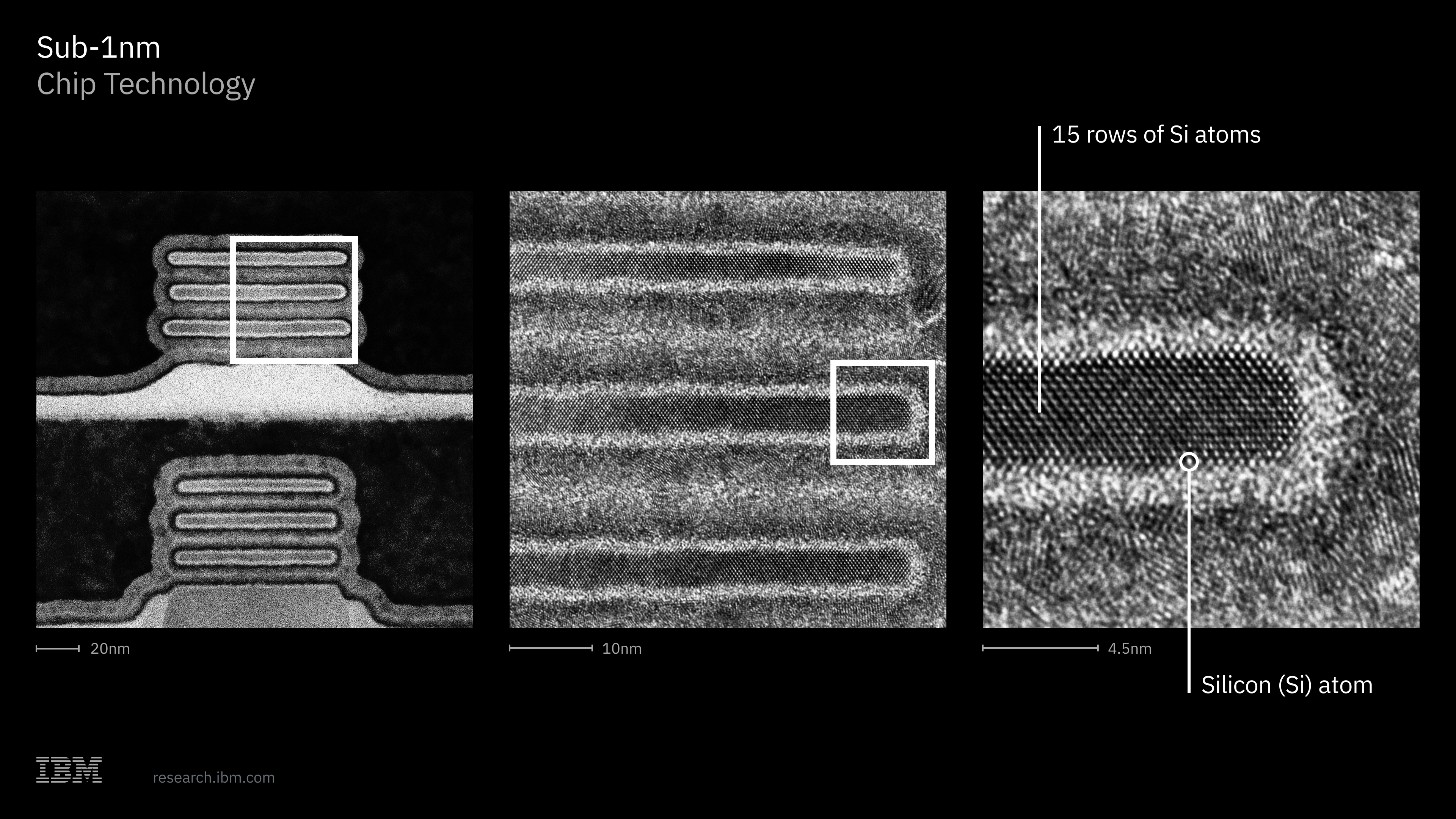
IBM’s new 0.7nm-class fabrication process uses nanostack transistors, requires 2x more FEOL steps for massive improvements in performance, power, and area.
TSMC has reportedly told customers to prepare for 5% to 10% price hikes across advanced chip nodes, extending beyond 3nm to include 7nm and some legacy processes.
I see your dancing robot and raise you a robot that can do actual work, live, while being streamed. Humanoid makers are getting real …
We just witnessed a significant semiconductor industry related non-cash trade deal take place on Twitter/X.
U.S. Commerce Secretary Lutnick expresses concerns in a conversation with ASML executives that China has an EUV lithography system as ASML denies shipping such scanners to the PRC.
…
Imec, ASML, and TSMC have integrated both n-type and p-type transistors with atomically thin 2D channels on a single 300mm wafer.
…
This roadmap provides an in-depth analysis of Intel’s current plans for its chip production capacity.
The NYT recently said it’s almost impossible to build robots without China. There are counter-examples very close to home, however …